Application and challenges of ruthenium in nanoscale integrated circuit interconnects
-
摘要:
随着集成电路工艺进入纳米尺度,传统铜互连面临电阻尺寸效应加剧和电迁移失效等问题,导致线电阻显著增加;同时,线间与层间电容的增强以及低介电材料的局限性共同引发寄生电容上升,进一步恶化了互连电容-电阻延迟问题。在此背景下,亟需探索新型互连材料并优化工艺以提升互连性能。钌作为下一代互连候选材料,凭借其较短的电子平均自由程和高内聚能,在纳米尺度下表现出低电阻尺寸效应和优异的抗电迁移特性。此外,钌具有良好的界面稳定性,无需扩散阻挡层即可实现工艺集成,并支持基于干法刻蚀的图形化处理,兼容半大马士革工艺及空气隙结构,从而能够有效降低互连结构的电阻和寄生电容。系统阐述了钌在纳米尺度下的量子输运机制、先进沉积技术及集成方案的研究进展,为后铜时代互连技术的发展提供理论支撑与技术路径参考。
Abstract:With the progression of integrated circuit technology into the nanoscale domain, conventional copper interconnects encounter growing challenges. These include increased resistivity due to size-dependent effects and electromigration-induced failures, which contribute to higher line resistance. Additionally, the rise in line-to-line and interlayer capacitance, compounded by the limitations of low dielectric constant materials, results in heightened parasitic capacitance and a corresponding degradation of interconnect RC delay. In response to these challenges, there is an urgent demand for innovative interconnect materials and refined processing techniques to enhance interconnect performance. Ruthenium (Ru), recognized as a promising candidate for next-generation interconnects, presents several inherent advantages at the nanoscale. Its short electron mean free path and high cohesive energy confer reduced resistivity scaling effects and superior electromigration resistance. Furthermore, Ru demonstrates excellent interfacial stability, eliminating the necessity for diffusion barrier layers. From a process integration standpoint, Ru facilitates dry etching-based patterning, ensuring compatibility with semi-damascene processes and air-gap structures, thus aiding in the reduction of both interconnect resistance and parasitic capacitance. This paper provides a comprehensive review of the quantum transport mechanisms of Ru at the nanoscale, recent advancements in deposition technologies, and integration strategies, offering theoretical insights and technological pathways for the advancement of post-Cu interconnect solutions.
-
0. 引言
在集成电路(IC)技术的发展进程中,晶体管数量在摩尔定律的推动下呈指数增长,极大地促进了前端工艺(FEOL)技术的演进与创新。然而,后端制程(BEOL)中互连结构的性能提升却相对滞后,成为制约芯片整体性能提升的关键瓶颈。互连结构通过复杂的布线连接数十亿个晶体管,其互连电阻(Resistance)与寄生电容(Capacitance)引起的RC延迟成为限制芯片工作频率的主要因素。传统上一般以铜(Cu)作为互连材料。当互连线宽低于Cu的电子平均自由程时,表面散射与晶界散射效应显著增强,会导致互连电阻的急剧上升[1-2]。与此同时,互连线截面积的显著减小会进一步加剧电子散射现象,电流密度和器件工作温度随之升高,进而引发电迁移或应力诱导的空洞问题,严重影响互连材料的可靠性。此外,随着互连关键尺寸的不断缩小,Cu互连对扩散阻挡层的依赖逐渐增大。由于阻挡层在沟槽中的占比逐步增加,导体的有效截面积被进一步压缩,不仅显著提升了互连电阻,还大幅增加了工艺复杂度[3-5]。
在此背景下,亟须探索具备低电阻尺寸效应和优异抗电迁移性能,并且与现有工艺制程兼容的新型互连材料。针对这一需求,研究者提出了多种替代金属材料,主要包括过渡金属(如钴[6-8]、钼[5,9-12]、镍)以及铂族金属(如钌、铑、铱)[13]等。其中,钴凭借较低的电阻率和良好的抗电迁移特性已成功应用于高密度逻辑器件的局部互连层,但其仍需扩散阻挡层以防止钴原子扩散,这在一定程度上提高了复杂性和成本[14-15]。钼具有成本优势,且在无阻挡层的情况下表现出较好的可靠性,但较高的电阻率限制了其在高性能互连中的应用[16-18]。在铂族金属中,钌(Ru)在纳米尺度下的电阻率相对较低,同时具备较高的内聚能(8.0 eV),因此在小尺寸互连中展现出电阻和抗电迁移方面的显著优势。此外,Ru在无阻挡层的情况下仍能保持良好的稳定性,从而简化了制造工艺[19]。这些特性使该材料在未来更先进的互补金属氧化物半导体(CMOS)技术节点中展现出广阔的应用前景,为5 nm以下集成电路性能的提升提供了重要的材料选择。
本文系统阐述Ru作为新一代互连材料的理论基础与技术进展。首先,基于量子输运理论阐述纳米互连的电阻尺寸效应,揭示Ru相较于Cu的本征优势;其次,探讨电迁移的物理机理,重点分析Ru作为新型互连金属在抑制电迁移方面的优异特性;再次,评述原子层沉积(ALD)技术在钌薄膜生长方面的研究进展及其在三维集成中的优势;最后,总结Ru在阻挡层与互连层中的应用现状及其发展前景。
1. 钌互连的优势
1.1 电阻的尺寸效应
在互连尺寸微缩过程中,当导线的线宽小于互连材料的电子平均自由程时,由于表面和晶界处的电子散射作用,其电阻率会迅速增加。例如,当铜互连的线宽缩小至10 nm时,其线电阻率相较于块体材料增加了约10倍[2-3]。这种金属电阻率的尺寸效应不仅导致功耗上升,还会引起信号延迟,从而对集成电路的进一步微缩造成障碍。
在块体材料中,电子的平均自由程主要由声子散射决定。然而,随着材料尺寸的减小,表面和晶界处的电子散射效应显著增强。根据经典Fuchs-Sondheimer(FS)模型[20]与Mayadas-Shatzkes(MS)模型[21-22],纳米导体的总电阻率(ρtotal)可表示为体电阻率(ρ0)、表面散射贡献(∆ρFS)以及晶界散射贡献(∆ρMS)的叠加,如式(1)[23]所示:
ρtotal=ρ0+ρ0λ3(1−p)4d+ρ0λ3R2D(1−R) (1) 式中,λ为电子平均自由程,p为表面散射参数,d为线宽,D为晶粒度,R为晶界反射系数。由此可见,纳米尺度导体的电阻率主要由3个关键变量共同决定:p、R以及本征导电品质因子(ρ0λ)。
FS模型通过表面散射参数p来区分漫散射(p=0)和镜面散射(p=1)。漫散射会导致电子动量随机化,从而显著增加电阻率;而在镜面散射过程中,平行于表面的动量分量得以保留,因此对电阻率的影响较小。参数p的值与互连金属的晶体取向及界面原子排列有序度密切相关,通过原子级平坦化工艺可将p值提升至接近1。
晶界散射效应与晶粒度(D)呈反比关系。当D远大于λ时,晶界散射的影响可以忽略不计;然而,当D与λ相当或小于λ时,晶界散射成为主导因素。通过退火和晶界掺杂处理,能够形成低能量的高对称晶界,从而减少电子反射并降低界面散射引起的电阻率上升[24]。
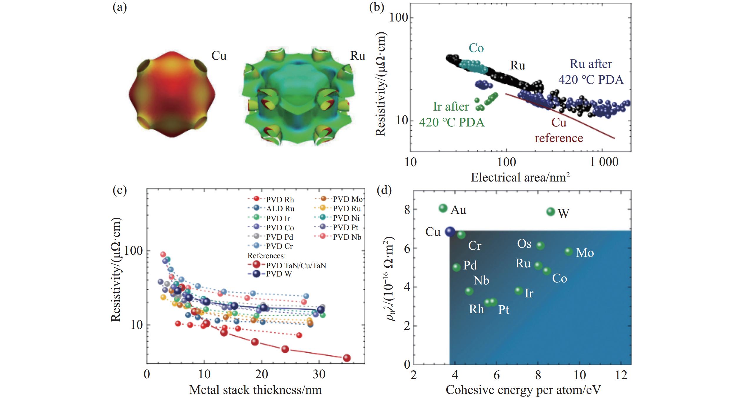
基于上述理论分析,以下结合图1和表1中的物理量,从表面散射参数、晶界反射系数和本征导电品质因子等3个方面探讨Ru在电阻尺寸效应方面的优势。相较于Cu具有的面心立方(fcc)结构,Ru的六方密排(hcp)结构具有原子级平整的(0001)晶面,因此镜面散射占主导,有利于降低表面散射对其电阻率的影响。此外,Ru的晶界对称性较高,费米面接近球形,使得电子更容易穿过晶界而不发生反射[24]。这种结构特性与晶界的低能量相结合,使Ru的晶界反射系数显著低于传统金属。从晶粒度来看,退火处理后Ru的晶粒度(20~50 nm)远大于其λ,从而将晶界散射的影响降至最低[25]。另外,尽管Ru的ρ0(7.8 μΩ·cm)高于Cu(1.68 μΩ·cm),但其λ远小于Cu,导致其ρ0λ值较低(表1)。理论计算表明,当线宽缩小至5 nm时,ρ0λ值每降低1×10⁻¹⁶ Ω·m2,总电阻率下降约35%[26]。综上所述,凭借优异的表面散射特性、低晶界散射以及较低的本征导电品质因子,Ru在纳米级互连中展现出显著优势,成为亚5 nm互连的理想候选材料。
![图 1 (a)Cu的面心立方和Ru的六方密排晶体结构示意图[13];(b)不同金属的电阻率与电学面积的关系[27];(c)金属薄膜的电阻率随厚度的变化趋势[28];(d)金属本征导电品质因子与单原子内聚能的关系[29]]() 图 1 (a)Cu的面心立方和Ru的六方密排晶体结构示意图[13];(b)不同金属的电阻率与电学面积的关系[27];(c)金属薄膜的电阻率随厚度的变化趋势[28];(d)金属本征导电品质因子与单原子内聚能的关系[29]Figure 1. (a) Schematic diagram of the face-centered cubic crystal structure of Cu and the hexagonal close-packed crystal structure of Ru[13]. (b) Resistivity versus electrical area for various metals[27]. (c) Trend of resistivity variation with thickness for metal-films[28]. (d) The relationship between the intrinsic conductivity figure of merit of metals (ρ0λ) and their cohesive energy[29]表 1 Cu与新型互连金属的材料特性Table 1. Material properties of Cu and novel interconnect metals
图 1 (a)Cu的面心立方和Ru的六方密排晶体结构示意图[13];(b)不同金属的电阻率与电学面积的关系[27];(c)金属薄膜的电阻率随厚度的变化趋势[28];(d)金属本征导电品质因子与单原子内聚能的关系[29]Figure 1. (a) Schematic diagram of the face-centered cubic crystal structure of Cu and the hexagonal close-packed crystal structure of Ru[13]. (b) Resistivity versus electrical area for various metals[27]. (c) Trend of resistivity variation with thickness for metal-films[28]. (d) The relationship between the intrinsic conductivity figure of merit of metals (ρ0λ) and their cohesive energy[29]表 1 Cu与新型互连金属的材料特性Table 1. Material properties of Cu and novel interconnect metals1.2 抗电迁移能力
随着集成电路制造工艺进入纳米尺度,电迁移引发的互连失效对器件可靠性造成了严重影响。电迁移现象源于导电电子与金属离子之间的动量交换作用。当电流密度超过阈值时,电子风作用力突破金属原子的扩散势垒,导致金属离子沿电子流方向发生定向迁移。如图2所示,这种质量输运失衡会在阴极区域形成微空洞,而在阳极区域造成原子堆积,最终导致互连结构出现开路或短路失效[30]。Black方程[31]定量描述了平均失效时间与电流密度的正相关性及其与激活能的负相关性,其中激活能主要由材料内聚能和扩散路径决定。
![图 2 (a)金属线中电迁移的物理机制[32];(b)Ru互连中电迁移引起晶界处(左)和电介质界面处(右)空洞的形成[33]]()
Cu因其较高的内聚能(3.8 eV)而具备较高的失效阈值电流密度[34-35],其电迁移行为以晶格扩散为主。然而,当Cu互连线宽缩减至亚10 nm时,晶界扩散显著加剧,从而加速了电迁移失效。尽管通过退火处理可形成竹节状晶粒结构以消除平行于电流方向的晶界[36],但在亚10 nm尺度下,晶粒分布的均匀性难以有效控制。
因此,为解决纳米金属互连中的电迁移问题,采用内聚能更高的Ru被认为是一种优选方案。因为较高的内聚能可增强原子间的结合力,从而减弱电子风力驱动的原子迁移,抑制电迁移的发生。此外,Ru的hcp晶体结构可有效降低晶格扩散系数,同时其晶界扩散势垒明显高于Cu,从而有效抑制快速扩散路径的形成。基于上述考虑,国际上已有多个关于Ru互连电迁移特性的报道[33, 37-38],如表2所示。测量温度相同时,与Cu互连相比,Ru互连在更细线宽和更高电流密度下可实现更长的失效时间。例如,Pedreira等[38]发现,10 nm宽Ru互连线在温度为330 ℃、电流密度为5 MA·cm−2的条件下,持续运行
1200 h后未出现失效现象。而在18 nm线宽下,在温度为330 ℃、电流密度为200 MA·cm−2的测试条件下,Ru互连的失效时间约为700 h[33],与Mo、Co互连[39-40]相比具有显著优势。表 2 Ru互连的电迁移失效测试与其他金属的对比Table 2. Electromigration failure tests of Ru interconnects compared with other metals2. Ru的原子层沉积
因其独特的材料本征特性,钌互连能够有效解决纳米尺度下电阻率急剧增加的问题,同时保持优异的抗电迁移性能。然而,在亚5 nm技术节点中,如何实现Ru薄膜在互连通孔中的无缝填充显得尤为重要。传统的物理气相沉积(PVD)工艺在填充小尺寸通孔时,容易在顶部侧壁形成悬垂结构或在底部附近产生空洞,这不仅会导致互连线电阻增大,还容易引发电迁移问题[41]。相比之下,原子层沉积技术凭借其卓越的台阶覆盖能力和厚度控制精度,成为纳米尺度互连结构制备的关键工艺。接下来,从前驱体的角度系统性地介绍钌的ALD生长工艺及其特性,具体内容如表3所示。根据钌前驱体中Ru的化合价状态,主要可分为0价、+2价以及更高价态(如+3价和+8价)的钌前驱体。
表 3 基于不同前驱体和反应物的Ru的ALD工艺汇总Table 3. Summary of ALD processes of Ru based on various precursors and reactants价态 前驱体 ALD工艺 反应物 基底 沉积温度/
℃孕育期/
循环电阻率/
(μΩ·cm)生长速率/
(nm·循环−1)参考
文献Ru(0) Ru(DMBD)(CO)3 TALD O2 SiO2、HfO2 260 ~0 9.1 0.050 [42] TALD O2 SiO2 255~280 ~0 14.0 0.067 [43] EBBDRu TALD O2 SiO2 225 15 26.0 0.056 [44] EBECHRu TALD O2 SiO2 250 ~5 18.0~22.0 0.148 [45] TALD O2 SiO2 140~350 3 24.0 0.042 [46] Ru(Ⅱ) RuCp2 TALD O2 SiO2、HfO2 310~350 — — 0.100 [47] TALD O2 SiO2/Al2O3
SiO2/TiO2275~400 250 13.0 0.045 [48] PEALD NH3 SiO2 300 ~0 14.0 0.120 [49] TALD O2 Si(TMA) — 25 — 0.045 [50] Ru(EtCp)2 PEALD NH3 SiO2 300 ~0 16.0 0.180 [49] PEALD NH3 SiO2/TiN 270 20 12.0 0.038 [51] PEALD O2 SiO2 200~400 ~0 18.2 0.036 [52] TALD O2 SiO2/TiN 270 — 15.0 0.150 [53] TALD O2 SiO2 300 200 — 0.049 [54] TALD O2 SiO2 275 ~0 15.0 0.060 [55] CpRu(CO)2Et PEALD O2 SiO2/TiN 325 45 16.0 0.100 [56] TALD O2 Si(TMA/DEZ) 300 20 — 0.100 [57] ((CH3)2C4H2N)2Ru TALD O2 SiO2、Al2O3 250~320 60 18.0~24.0 0.022 [58] (C2H5C5H4)(NC4H4)Ru TALD O2 SiO2、TiN 275~350 50 21.6 0.047 [59] Ru(Ⅲ) Ru(thd)3 TALD O2 Al2O3 325~450 250 15.0~20.0 0.036 [60] Ru(Ⅷ) RuO4 PEALD H2 H-Si 50~100 — 18.0 0.100~0.120 [61] RuO4 TALD H2 H-Si 100 — 20.0 — [61] RuO4 TALD H2 Si/Ta2O5 140~230 — 23.0 0.022 [62] 0价Ru前驱体(Ru(0))因其独特的化学特性而展现出显著的工艺优势。Ru(0)无需经历表面还原反应,可直接通过化学吸附实现原子层沉积,从而大幅简化工艺流程。这一特性使0价前驱体在成核初期表现出优异的界面结合能力,几乎不存在成核延迟,并且能够在SiO2等惰性衬底上实现瞬时连续生长,有效避免了传统工艺中岛状成核导致的界面粗糙问题。以Ru(DMBD)(CO)3前驱体为例,采用热原子层沉积(TALD)工艺制备Ru薄膜时,几乎观察不到成核延迟现象;对生长的薄膜在500 ℃温度下、H2/N2混合气氛中进行退火,其电阻率可降至9.1 μΩ·cm,接近Ru的理论电阻率(7.1 μΩ·cm)[42]。其原因在于,退火有效去除了薄膜中残留的杂质(如C、O),并且高温促使Ru晶粒度增大,从而降低了晶界散射对电子运动的阻碍作用。然而,基于Ru(0)前驱体的TALD生长仍然存在生长速率偏低的问题,大多约为0.05 nm·循环−1[42, 44, 46]。为提升薄膜的沉积速率,通过增加工艺压力来降低Ru成核的临界尺寸和活化能,将生长速率提升至0.148 nm·循环−1[45]。
2价Ru前驱体(Ru(II))主要包括RuCp2、Ru(EtCp)2以及CpRu(CO)2Et等。Aaltonen等[48]采用TALD工艺,以RuCp2为前驱体,O2为反应物,在275~400 ℃沉积温度范围内实现了0.045 nm·循环−1的生长速率,其中在350 ℃下生长的Ru薄膜的电阻率低至13 μΩ·cm。然而,该工艺存在明显的不足:一方面,较低的生长速率导致成膜效率受限;另一方面,在SiO2等惰性衬底上出现严重的成核延迟现象,需要超过250个循环才能形成连续薄膜。针对上述问题,Park等[49]采用等离子体增强ALD(PEALD)技术,以NH3等离子体替代O2作为反应物,显著抑制了成核延迟,同时将生长速率提升至0.12 nm·循环−1;进一步研究表明,采用液态前驱体Ru(EtCp)2可发挥其高蒸气压和高热稳定性的优势,在PEALD工艺中实现无成核延迟的Ru薄膜沉积,将生长速率进一步提升至0.18 nm·循环−1。对于RuCp2前驱体引起的成核密度不足问题,表面预处理技术可有效解决。例如,通过三甲基铝(TMA)或二乙基锌(DEZ)预处理SiO2衬底,可使其表面化学吸附位点密度增加2.5倍,将成核延迟时间缩短至25个循环以下[50]。然而,该方案的薄膜生长速率仍然较低(0.045 nm·循环−1)。为此,采用具有新型配体的前驱体CpRu(CO)2Et,可以在保持预处理技术优势的同时,将生长速率提升至0.11 nm·循环−1[57]。
高价态Ru前驱体(如Ru(Ⅲ)和Ru(Ⅷ))因其高氧化还原活性,在ALD工艺中也展现出一定优势。例如,Ru(thd)3适用于高温(325~450 ℃)沉积,但生长速率偏低,仅为0.036 nm·循环−1[60]。RuO4与H2等离子体在50~100 ℃低温区间沉积时,可以达到0.11 nm·循环−1的生长速率[61]。这是由于RuO4的强氧化性可确保前驱体分子在表面发生完全分解,所制备的Ru薄膜杂质含量极低,显著优于基于2价钌前驱体的结果。然而,RuO4具有剧毒且热稳定性差,在工艺中需精确控制还原气体的比例,因此限制了其在工业中的广泛应用。
在目前的Ru薄膜ALD技术中,可以通过工艺优化、衬底表面预处理、前驱体配体结构设计及其价态选择等方式,提升Ru薄膜的生长速率,降低成核延迟和电阻率,从而推动Ru薄膜在亚5 nm技术节点中的应用。
3. Ru互连的应用
Ru作为一种新型互连材料,因其优异的阻挡性能和导电特性,在先进节点中展现出独特的应用潜力。
3.1 阻挡层
在先进互连技术节点中,传统Ta/TaN阻挡层体系面临严峻挑战。Ru因其独特的物理化学特性成为新一代Cu互连扩散阻挡层的理想候选材料。一方面,Ru的电阻率仅为TaN的1/25,且具有低电阻尺寸效应,有利于降低互连线路的整体电阻;另一方面,Ru凭借其较高的熔点和内聚能,可有效抑制高温工艺中的原子互扩散。此外,Ru还可作为电化学镀铜的籽晶层,可通过ALD工艺生长实现在高深宽比沟槽中的均匀覆盖。因此,研究者们针对Ru基阻挡层进行了大量研究。
早期的研究主要采用PVD技术来制备Ru薄膜。例如,20 nm厚的Ru薄膜可有效抑制450 ℃退火时Cu向Si衬底的扩散[63]。然而,当Ru膜厚度缩减至5 nm时,Cu/Ru/Si结构在经历450 ℃退火后,因形成Ru2Si3界面层而导致阻挡层失效[64]。为了突破超薄Ru阻挡层的局限性,一方面可以在Ru/Si界面处插入5 nm非晶TaN,以阻止Ru与Si的直接反应并阻断Cu沿晶界的扩散[65],从而使阻挡层失效温度提升至750 ℃;另一方面,可以采用合金化或掺杂方式,利用晶界填充效应或非晶结构来提高阻挡性能。例如,在Ru中掺杂W形成的非晶阻挡层薄膜在650 ℃时能阻止Cu的渗透,且在Ta基板上的润湿角比Cu更低,有利于薄膜的沉积和覆盖[66]。对于在Ru中掺入5% Cr形成的非晶Ru-Cr薄膜,可有效抑制晶界扩散,将其失效温度提升至650 ℃,同时还增强了Ru的黏附性[67]。此外,通过ALD工艺制备的5 nm Ru-Mn薄膜,在经历600 ℃退火后,Mn迁移至界面形成2 nm厚的MnSiOx层,有助于保持完整的界面特性[68]。PVD制备的5 nm Ru-Mo薄膜与纯Ru薄膜相比,失效温度可提高175 ℃,并且在725 ℃的退火温度下具有更好的阻挡效果[69]。作为阻挡层材料的RuTa或RuTa(N)具有优异的取向特性,因而在Cu(111)晶面上具有更好的润湿性和填充能力,从而降低了界面电阻并提高了抗电迁移能力,延长了互连寿命[70]。电镀Ru-Co合金则结合Ru与Co的协同效应,在400 ℃退火后仍保持完整的叠层结构[71]。
总的来说,通过界面优化和非晶化材料设计,Ru基阻挡层实现了阻挡性能与工艺兼容性的双重突破。
3.2 互连线
随着集成电路工艺节点持续微缩至亚5 nm,基于Cu的局域互连面临巨大挑战。一方面,在电镀法沉积Cu薄膜过程中,Cu电镀液中常用的大分子添加剂在通孔侧壁形成的吸附层可能引发纳米级孔道阻塞,从而抑制Cu离子的有效传输,导致沟槽填充不完全。另一方面,Cu互连依赖的扩散阻挡层厚度难以进一步减小,从而在局域互连通孔中占据大量空间。这些因素将加剧互连电阻的提升和可靠性的恶化,成为制约先进互连工艺性能提升的关键瓶颈。因此,国际上提出了一种基于Ru的半大马士革互连方案,以替代传统的铜/扩散阻挡层技术路线。
Ru半大马士革互连的关键工艺流程如图3(a)所示,主要包括3个步骤:首先进行通孔刻蚀,随后依次沉积Ru金属和硬掩膜层,最终通过干法刻蚀工艺实现Ru金属线的精确图形化。该工艺通过直接金属刻蚀形成面内互连结构,避免了传统双大马士革互连工艺中的通孔和沟槽填充难题。因此,这种半大马士革互连工艺不仅能够提升线高的控制精度,还可实现更大深宽比(6~8)的金属线,从而有助于降低互连电阻。据报道[72],在18 nm金属间距与10 nm关键尺寸条件下,Ru半大马士革互连的线电阻相较于Cu双大马士革互连降低了75%。
![图 3 (a)半大马士革工艺流程[78];(b)带气隙结构的Ru半大马士革互连线结构[79];(c)Cu双大马士革工艺、带气隙结构的Ru半大马士革工艺及Ru半大马士革工艺在不同深宽比沟槽下的RC延迟[72];Ru Top Via结构的(d)工艺流程以及(e)横截面透射电子显微镜图像[75]]() 图 3 (a)半大马士革工艺流程[78];(b)带气隙结构的Ru半大马士革互连线结构[79];(c)Cu双大马士革工艺、带气隙结构的Ru半大马士革工艺及Ru半大马士革工艺在不同深宽比沟槽下的RC延迟[72];Ru Top Via结构的(d)工艺流程以及(e)横截面透射电子显微镜图像[75]Figure 3. (a) Process flow of the semi-damascene technique[78]. (b) Ru semi-damascene interconnect structure incorporating an air-gap design[79]. (c) The RC delay characteristics of the Cu dual-damascene process, air-gap integrated Ru semi-damascene process, and Ru semi-damascene process under varying trench aspect ratios[72]. (d) Process flow of the Ru Top Via structure[75]. (e) Cross-sectional transmission electron microscopy (TEM) image of the Ru Top Via structure[75]
图 3 (a)半大马士革工艺流程[78];(b)带气隙结构的Ru半大马士革互连线结构[79];(c)Cu双大马士革工艺、带气隙结构的Ru半大马士革工艺及Ru半大马士革工艺在不同深宽比沟槽下的RC延迟[72];Ru Top Via结构的(d)工艺流程以及(e)横截面透射电子显微镜图像[75]Figure 3. (a) Process flow of the semi-damascene technique[78]. (b) Ru semi-damascene interconnect structure incorporating an air-gap design[79]. (c) The RC delay characteristics of the Cu dual-damascene process, air-gap integrated Ru semi-damascene process, and Ru semi-damascene process under varying trench aspect ratios[72]. (d) Process flow of the Ru Top Via structure[75]. (e) Cross-sectional transmission electron microscopy (TEM) image of the Ru Top Via structure[75]半大马士革工艺的另一核心优势在于其与气隙(Airgap)工艺的兼容性,如图3(b)所示。由于该工艺可在金属线刻蚀完成后进行介质填充,因此能够在间距较窄的面内互连线间引入气隙(介电常数k=1),从而降低互连线间的寄生电容。同时,还避免了大马士革工艺中低k介质因等离子体损伤而引起的寄生电容增大问题。如图3(c)所示,相比于深宽比为2的Cu双大马士革互连,Ru半大马士革互连的RC延迟降低了24%。结合Airgap结构并将深宽比增加到6,可使RC延迟进一步降低68%[72]。此外,在ARM 64位CPU设计基准的实际测试中,相较于深宽比为3的Cu双大马士革互连,结合Airgap方案的Ru半大马士革互连实现了频率提升15%和功耗降低10%的显著效果[73]。在可靠性方面,宽度为14 nm并结合Airgap结构的Ru互连线在温度为330 ℃、电流密度为5 MA·cm−2的条件下,经过
1200 h测试后未观测到电阻漂移或界面分层现象[74]。在Ru半大马士革工艺的基础上,顶部通孔(Top Via)结构的引入及其工艺优势显著推动了后铜互连技术的微缩化。如图3(d)和(e)所示,该工艺凭借通孔与下层线路的自对准集成实现同步金属化,结合改进的间隔物辅助光刻蚀刻光刻(spacer assisted litho-etch litho-etch, SALELE)工艺,使18 nm极窄节距的Ru互连图案化成为可能[75-77]。此外,顶部通孔结构结合Airgap可显著降低互连电容。实验结果表明,通过优化Airgap占沟槽高度的比例,Top Via可在18 nm金属间距下将线间寄生电容降低23%。在可靠性评估中,对采用Top Via工艺的Airgap Ru互连线(Ru长度为60 μm)进行了电迁移测试。测试温度和电流密度分别为380 ℃和20 MA·cm−2。结果表明,在700 h 内,基本未出现电迁移失效现象[76]。综上所述,Ru 的Top Via工艺通过对图案化技术、气隙集成以及自对准通孔设计的协同优化,在RC性能与可靠性方面均展现出显著优势,为Cu互连技术提供了可行的替代方案。
4. 挑战与展望
尽管钌作为下一代互连材料在纳米尺度集成电路中展现出显著优势,但其实际应用仍面临诸多挑战。首先,ALD工艺的优化有待突破。PEALD工艺在降低成核延迟期的同时,会导致薄膜表面粗糙度的提升;0价前驱体虽能增加成核密度,但成本较高。此外,Ru薄膜的电阻率通常高于理论值,尽管能够通过后续高温退火进行改善,但可能导致热预算增加。其次,Ru与低k介质之间的界面黏附性不足,会影响在作为阻挡层和互连线过程中互连结构的可靠性。最后,图形化工艺的精度与均匀性面临挑战。在半大马士革工艺中,高深宽比结构的干法刻蚀容易导致线边缘粗糙度和电阻非均匀性的提高,尤其在亚5 nm技术节点下,刻蚀选择比和侧壁形貌控制成为关键瓶颈。此外,气隙机械结构在动态应力或热循环下可能产生裂纹,需通过应力工程或界面强化提高其耐久性。
针对以上挑战,未来研究需聚焦于以下方向:一是优化ALD工艺,通过开发高活性前驱体与等离子体辅助技术,提升薄膜生长速率,降低杂质含量,开发高质量Ru薄膜的沉积工艺,以满足局部互连的填充需求;二是改善Ru与低k介质之间的界面黏附性,通过引入黏附层或进行表面修饰,提升界面结合强度,以保障互连结构的长期可靠性。上述技术突破将为Ru互连材料的规模化应用奠定基础,助力下一代高性能集成电路的发展。
-
![]()
图 1 (a)Cu的面心立方和Ru的六方密排晶体结构示意图[13];(b)不同金属的电阻率与电学面积的关系[27];(c)金属薄膜的电阻率随厚度的变化趋势[28];(d)金属本征导电品质因子与单原子内聚能的关系[29]
Figure 1. (a) Schematic diagram of the face-centered cubic crystal structure of Cu and the hexagonal close-packed crystal structure of Ru[13]. (b) Resistivity versus electrical area for various metals[27]. (c) Trend of resistivity variation with thickness for metal-films[28]. (d) The relationship between the intrinsic conductivity figure of merit of metals (ρ0λ) and their cohesive energy[29]
![]()
![]()
图 3 (a)半大马士革工艺流程[78];(b)带气隙结构的Ru半大马士革互连线结构[79];(c)Cu双大马士革工艺、带气隙结构的Ru半大马士革工艺及Ru半大马士革工艺在不同深宽比沟槽下的RC延迟[72];Ru Top Via结构的(d)工艺流程以及(e)横截面透射电子显微镜图像[75]
Figure 3. (a) Process flow of the semi-damascene technique[78]. (b) Ru semi-damascene interconnect structure incorporating an air-gap design[79]. (c) The RC delay characteristics of the Cu dual-damascene process, air-gap integrated Ru semi-damascene process, and Ru semi-damascene process under varying trench aspect ratios[72]. (d) Process flow of the Ru Top Via structure[75]. (e) Cross-sectional transmission electron microscopy (TEM) image of the Ru Top Via structure[75]
表 2 Ru互连的电迁移失效测试与其他金属的对比
Table 2 Electromigration failure tests of Ru interconnects compared with other metals
 下载: 导出CSV
表 3 基于不同前驱体和反应物的Ru的ALD工艺汇总
Table 3 Summary of ALD processes of Ru based on various precursors and reactants
价态 前驱体 ALD工艺 反应物 基底 沉积温度/
℃孕育期/
循环电阻率/
(μΩ·cm)生长速率/
(nm·循环−1)参考
文献Ru(0) Ru(DMBD)(CO)3 TALD O2 SiO2、HfO2 260 ~0 9.1 0.050 [42] TALD O2 SiO2 255~280 ~0 14.0 0.067 [43] EBBDRu TALD O2 SiO2 225 15 26.0 0.056 [44] EBECHRu TALD O2 SiO2 250 ~5 18.0~22.0 0.148 [45] TALD O2 SiO2 140~350 3 24.0 0.042 [46] Ru(Ⅱ) RuCp2 TALD O2 SiO2、HfO2 310~350 — — 0.100 [47] TALD O2 SiO2/Al2O3
SiO2/TiO2275~400 250 13.0 0.045 [48] PEALD NH3 SiO2 300 ~0 14.0 0.120 [49] TALD O2 Si(TMA) — 25 — 0.045 [50] Ru(EtCp)2 PEALD NH3 SiO2 300 ~0 16.0 0.180 [49] PEALD NH3 SiO2/TiN 270 20 12.0 0.038 [51] PEALD O2 SiO2 200~400 ~0 18.2 0.036 [52] TALD O2 SiO2/TiN 270 — 15.0 0.150 [53] TALD O2 SiO2 300 200 — 0.049 [54] TALD O2 SiO2 275 ~0 15.0 0.060 [55] CpRu(CO)2Et PEALD O2 SiO2/TiN 325 45 16.0 0.100 [56] TALD O2 Si(TMA/DEZ) 300 20 — 0.100 [57] ((CH3)2C4H2N)2Ru TALD O2 SiO2、Al2O3 250~320 60 18.0~24.0 0.022 [58] (C2H5C5H4)(NC4H4)Ru TALD O2 SiO2、TiN 275~350 50 21.6 0.047 [59] Ru(Ⅲ) Ru(thd)3 TALD O2 Al2O3 325~450 250 15.0~20.0 0.036 [60] Ru(Ⅷ) RuO4 PEALD H2 H-Si 50~100 — 18.0 0.100~0.120 [61] RuO4 TALD H2 H-Si 100 — 20.0 — [61] RuO4 TALD H2 Si/Ta2O5 140~230 — 23.0 0.022 [62]
下载: 导出CSV
-
[1] TIMALSINA Y P, HORNING A, SPIVEY R F, et al. Effects of nanoscale surface roughness on the resistivity of ultrathin epitaxial copper films[J]. Nanotechnology, 2015, 26(7): 075704. DOI: 10.1088/0957-4484/26/7/075704
[2] JOSELL D, BRONGERSMA S H, TOKEI Z. Size-dependent resistivity in nanoscale interconnects[J]. Annual Review of Materials Research, 2009, 39(1): 231-254. DOI: 10.1146/annurev-matsci-082908-145415
[3] GRAHAM R L, ALERS G B, MOUNTSIER T, et al. Resistivity dominated by surface scattering in sub-50 nm Cu wires[J]. Applied Physics Letters, 2010, 96(4): 042116. DOI: 10.1063/1.3292022
[4] PAN C, NAEEMI A. A proposal for a novel hybrid interconnect technology for the end of roadmap[J]. IEEE Electron Device Letters, 2013, 35(2): 250-252.
[5] GALL D. Metals for low-resistivity interconnects[C]// Proceedings of the 2018 IEEE International Interconnect Technology Conference (IITC). New York: IEEE, 2018: 157-159.
[6] AUTH C, ALIYARUKUNJU A, ASORO M, et al. A 10 nm high performance and low power CMOS technology featuring 3rd generation FinFET transistors, self-aligned quad patterning, contact over active gate and cobalt local interconnects[C]//Proceedings of the 2017 IEEE International Electron Devices Meeting (IEDM). New York: IEEE, 2017: 29.1.1-29.1.4.
[7] YEOH A, MADHAVAN A, KYBERT N, et al. Interconnect stack using self-aligned quad and double patterning for 10 nm high-volume manufacturing[C]//Proceedings of the 2018 IEEE International Interconnect Technology Conference (IITC). New York: IEEE, 2018: 144-147.
[8] GRIGGIO F, PALMER J, PAN F, et al. Reliability of dual-damascene local interconnects featuring cobalt on 10 nm logic technology[C]//Proceedings of the 2018 IEEE International Reliability Physics Symposium (IRPS). New York: IEEE, 2018: 6E.3-1-6E.3-5.
[9] ADELMANN C, WEN L G, PETER A P, et al. Alternative metals for advanced interconnects[C]//Proceedings of the 2014 IEEE International Interconnect Technology Conference (IITC). New York: IEEE, 2014: 173-176.
[10] KIM J, RHEE H, SON M W, et al. Electromigration reliability of barrierless Ruthenium and molybdenum for sub-10 nm interconnection[J]. ACS Applied Electronic Materials, 2023, 5(5): 2447-2453. DOI: 10.1021/acsaelm.3c00070
[11] GALL D. Electron mean free path in elemental metals[J]. Journal of Applied Physics, 2016, 119(8): 085101. DOI: 10.1063/1.4942216
[12] FOUNTA V, SOULIÉ J P, SANKARAN K, et al. Properties of ultrathin molybdenum films for interconnect applications[J]. Materialia, 2022, 24: 101511. DOI: 10.1016/j.mtla.2022.101511
[13] DUTTA S, SANKARAN K, MOORS K, et al. Thickness dependence of the resistivity of platinum-group metal thin films[J]. Journal of Applied Physics, 2017, 122(2): 025107. DOI: 10.1063/1.4992089
[14] TIERNO D, PEDREIRA O V, WU C, et al. Cobalt and ruthenium drift in ultra-thin oxides[J]. Microelectronics Reliability, 2019, 100: 113407.
[15] TIERNO D, LESNIEWSKA A, KLJUCAR L, et al. Impact of surface condition on cobalt drift into LK3.0 films[C]//Proceedings of the 2020 IEEE International Interconnect Technology Conference (IITC). New York: IEEE, 2020: 142-144.
[16] GUPTA A, MAES J W, JOURDAN N, et al. Barrierless ALD molybdenum for buried power rail and via-to-buried power rail metallization[C]//Proceedings of the 2022 IEEE International Interconnect Technology Conference (IITC). New York: IEEE, 2022: 58-60.
[17] HOSSEINI M, TIERNO D, MAES J W, et al. ALD Mo for advanced MOL local interconnects[C]//Proceedings of the 2022 IEEE International Interconnect Technology Conference (IITC). New York: IEEE, 2022: 145-147.
[18] DECOSTER S, CAMEROTTO E, MURDOCH G, et al. Patterning challenges for direct metal etch of ruthenium and molybdenum at 32 nm metal pitch and below [J]. Journal of Vacuum Science & Technology B, 2022, 40(3): 032802
[19] WAN D, PAOLILLO S, RASSOUL N, et al. Subtractive etch of ruthenium for sub-5 nm interconnect[C]//Proceedings of the 2018 IEEE International Interconnect Technology Conference (IITC). New York: IEEE, 2018: 10-12.
[20] FUCHS K. The conductivity of thin metallic films according to the electron theory of metals[J]. Mathematical Proceedings of the Cambridge Philosophical Society, 1938, 34(1): 100-108.
[21] MAYADAS A F, SHATZKES M, JANAK J F. Electrical resistivity model for polycrystalline films: the case of specular reflection at external surfaces[J]. Applied Physics Letters, 1969, 14(11): 345-347. DOI: 10.1063/1.1652680
[22] MAYADAS A F, SHATZKES M. Electrical-resistivity model for polycrystalline films: the case of arbitrary reflection at external surfaces[J]. Physical Review B, 1970, 1(4): 1382-1389. DOI: 10.1103/PhysRevB.1.1382
[23] GALL D. The search for the most conductive metal for narrow interconnect lines[J]. Journal of Applied Physics, 2020, 127(5): 050901. DOI: 10.1063/1.5133671
[24] CESAR M, GALL D, GUO H. Reducing grain-boundary resistivity of copper nanowires by doping[J]. Physical Review Applied, 2016, 5(5): 054018. DOI: 10.1103/PhysRevApplied.5.054018
[25] KOTSUGI Y, HAN S M, KIM Y H, et al. Atomic layer deposition of Ru for replacing Cu-interconnects[J]. Chemistry of Materials, 2021, 33(14): 5639-5651. DOI: 10.1021/acs.chemmater.1c01054
[26] MILOSEVIC E, KERDSONGPANYA S, ZANGIABADI A, et al. Resistivity size effect in epitaxial Ru(0001) layers[J]. Journal of Applied Physics, 2018, 124(16): 165105. DOI: 10.1063/1.5046430
[27] CROES K, ADELMANN C, WILSON C J, et al. Interconnect metals beyond copper: reliability challenges and opportunities[C]//Proceedings of the 2018 IEEE International Electron Devices Meeting (IEDM). New York: IEEE, 2018: 5.3.1-5.3.4.
[28] POPOVICI M, GROVEN B, MARCOEN K, et al. Atomic layer deposition of ruthenium thin films from (ethylbenzyl)(1-ethyl-1, 4-cyclohexadienyl) Ru: process characteristics, surface chemistry, and film properties[J]. Chemistry of Materials, 2017, 29(11): 4654-4666. DOI: 10.1021/acs.chemmater.6b05437
[29] ADELMANN C, SANKARAN K, DUTTA S, et al. Alternative metals: from ab initio screening to calibrated narrow line models[C]//Proceedings of the 2018 IEEE International Interconnect Technology Conference (IITC). New York: IEEE, 2018: 154-156.
[30] GUI X, HASLETT J W, DEW S K, et al. Simulation of temperature cycling effects on electromigration behavior under pulsed current stress[J]. IEEE Transactions on Electron Devices, 1998, 45(2): 380-386. DOI: 10.1109/16.658670
[31] BLACK J R. Electromigration—a brief survey and some recent results[J]. IEEE Transactions on Electron Devices, 1969, 16(4): 338-347. DOI: 10.1109/T-ED.1969.16754
[32] CAI L, CHEN Y, ZHANG H, et al. Insight into electromigration reliability of buried power rail with alternative metal material[J]. IEEE Transactions on Electron Devices, 2023, 71(1): 418-424.
[33] PEDREIRA O V, STUCCHI M, GUPTA A, et al. Metal reliability mechanisms in Ruthenium interconnects[C]// Proceedings of the 2020 IEEE International Reliability Physics Symposium (IRPS). New York: IEEE, 2020: 1-7.
[34] ROSENBERG R, EDELSTEIN D C, HU C K, et al. Copper metallization for high performance silicon technology[J]. Annual Review of Materials Science, 2000, 30(1): 229-262. DOI: 10.1146/annurev.matsci.30.1.229
[35] ANDRICACOS P C. Copper on-chip interconnections: a breakthrough in electrodeposition to make better chips[J]. The Electrochemical Society Interface, 1999, 8(1): 32-37. DOI: 10.1149/2.F06991IF
[36] HU C K, GIGNAC L, LIAN G, et al. Mechanisms of electromigration damage in Cu interconnects[C]// Proceedings of the 2018 IEEE International Electron Devices Meeting (IEDM). New York: IEEE, 2018: 5.2.1-5.2.4.
[37] HU C K, KELLY J, HUANG H, et al. Future on-chip interconnect metallization and electromigration[C]// Proceedings of the 2018 IEEE International Reliability Physics Symposium (IRPS). New York: IEEE, 2018: 4F.1-1-4F.1-6.
[38] PEDREIRA O V, CROES K, LEŚNIEWSKA A, et al. Reliability study on cobalt and ruthenium as alternative metals for advanced interconnects[C]//Proceedings of the 2017 IEEE International Reliability Physics Symposium (IRPS). New York: IEEE, 2017: 6B-2.1-6B-2.8.
[39] GUPTA A, RADISIC D, MAES J W, et al. Buried power rail metal exploration towards the 1 nm node[C]//Proceedings of the 2021 IEEE International Electron Devices Meeting (IEDM). New York: IEEE, 2021: 22.5.1-22.5.4.
[40] PEDREIRA O V, LOFRANO M, ZAHEDMANESH H, et al. Assessment of critical Co electromigration parameters for the 1 nm node[C]//Proceedings of the 2022 IEEE International Reliability Physics Symposium (IRPS). New York: IEEE, 2022: 8C.2-1-8C.2-7.
[41] MEVELLEC V, THIAM M, SUHR D, et al. A novel bottom-up fill mechanism for the metallization of advanced node copper interconnects[J]. ECS Transactions, 2016, 75(7): 9-14. DOI: 10.1149/07507.0009ecst
[42] HAYES M H, JENKINS M A, WOODRUFF J, et al. Improved properties of atomic layer deposited ruthenium via post-deposition annealing[J]. Journal of Vacuum Science & Technology A, 2021, 39(5): 052402.
[43] AUSTIN D Z, JENKINS M A, ALLMAN D, et al. Atomic layer deposition of ruthenium and ruthenium oxide using a zero-oxidation state precursor[J]. Chemistry of Materials, 2017, 29(3): 1107-1115. DOI: 10.1021/acs.chemmater.6b04251
[44] YEO S, PARK J Y, LEE S J, et al. Ruthenium and ruthenium dioxide thin films deposited by atomic layer deposition using a novel zero-valent metal-organic precursor, (ethylbenzene)(1, 3-butadiene) Ru(0), and molecular oxygen[J]. Microelectronic Engineering, 2015, 137: 16-22. DOI: 10.1016/j.mee.2015.02.026
[45] KANG N G, HA M J, AHN J H, et al. Ultrathin metal films with low resistivity via atomic layer deposition: process pressure effect on initial growth behavior of Ru films[J]. Chemistry of Materials, 2024, 36(17): 8496-8503. DOI: 10.1021/acs.chemmater.4c01707
[46] HONG T E, CHOI S H, YEO S, et al. Atomic layer deposition of Ru thin films using a Ru(0) metallorganic precursor and O2[J]. ECS Journal of Solid State Science and Technology, 2012, 2(3): 47-53.
[47] PARK K J, DOUB J M, GOUGOUSI T, et al. Microcontact patterning of ruthenium gate electrodes by selective area atomic layer deposition[J]. Applied Physics Letters, 2005, 86(5): 051903. DOI: 10.1063/1.1852079
[48] AALTONEN T, ALEN P, RITALA M, et al. Ruthenium thin films grown by atomic layer deposition[J]. Chemical Vapor Deposition, 2003, 9(1): 45-49. DOI: 10.1002/cvde.200290007
[49] PARK S J, KIM W H, MAENG W J, et al. Thermal and plasma enhanced atomic layer deposition ruthenium and electrical characterization as a metal electrode[J]. Microelectronic Engineering, 2008, 85(1): 39-44. DOI: 10.1016/j.mee.2007.01.239
[50] ROTHMAN A, WERBROUCK A, BENT S F, et al. Enhanced growth in atomic layer deposition of ruthenium metal: the role of surface diffusion and nucleation sites[J]. Chemistry of Materials, 2023, 36(1): 541-550.
[51] KWON O K, KWON S H, PARK H S, et al. PEALD of a ruthenium adhesion layer for copper interconnects[J]. Journal of The Electrochemical Society, 2004, 151(12): C753-C756. DOI: 10.1149/1.1809576
[52] ROGOZHIN A, MIAKONKIKH A, SMIRNOVA E, et al. Plasma enhanced atomic layer deposition of ruthenium films using Ru(EtCp)2 precursor[J]. Coatings, 2021, 11(2): 117. DOI: 10.3390/coatings11020117
[53] KWON O K, KIM J H, PARK H S, et al. Atomic layer deposition of ruthenium thin films for copper glue layer[J]. Journal of the Electrochemical Society, 2004, 151(2): G109-G112. DOI: 10.1149/1.1640633
[54] YIM S S, LEE D J, KIM K S, et al. Nucleation kinetics of Ru on silicon oxide and silicon nitride surfaces deposited by atomic layer deposition[J]. Journal of Applied Physics, 2008, 103(11): 113509. DOI: 10.1063/1.2938052
[55] CHEN Z, HUANG F, WANG B, et al. Atomic layer deposition of Ru in nanoTSV with high coverage and low resistivity[J]. Nanoscale Advances, 2025, 7: 1-7. DOI: 10.1039/D5NA90001H
[56] LEICK N, VERKUIJLEN R O F, LAMAGNA L, et al. Atomic layer deposition of Ru from CpRu(CO)2Et using O2 gas and O2 plasma[J]. Journal of Vacuum Science & Technology A, 2011, 29(2): 021016.
[57] ROTHMAN A, SEO S, WOODRUFF J, et al. Enhanced nucleation mechanism in ruthenium atomic layer deposition: exploring surface termination and precursor ligand effects with RuCpEt(CO)2[J]. Journal of Vacuum Science & Technology A, 2024, 42(5): 052402.
[58] KUKLI K, AARIK J, AIDLA A, et al. Atomic layer deposition of Ru films from bis(2, 5-dimethylpyrrolyl) ruthenium and oxygen[J]. Thin Solid Films, 2012, 520(7): 2756-2763. DOI: 10.1016/j.tsf.2011.11.088
[59] KUKLI K, KEMELL M, PUUKILAINEN E, et al. Atomic layer deposition of ruthenium films from (ethylcyclopentadienyl)(pyrrolyl) ruthenium and oxygen[J]. Journal of The Electrochemical Society, 2011, 158(3): D158-D165. DOI: 10.1149/1.3533387
[60] AALTONEN T, RITALA M, ARSTILA K, et al. Atomic layer deposition of ruthenium thin films from Ru(thd)3 and oxygen[J]. Chemical Vapor Deposition, 2004, 10(4): 215-219. DOI: 10.1002/cvde.200306288
[61] MINJAUW M, DENDOOVEN J, CAPON B, et al. Low temperature thermal and plasma enhanced atomic layer deposition of ruthenium using RuO4 and H2/H2-plasma[C]//Proceedings of the 2015 IEEE International Interconnect Technology Conference and 2015 IEEE Materials for Advanced Metallization Conference (IITC/MAM). New York: IEEE, 2015: 33-36.
[62] AN C H, KIM S H, KWON D S, et al. Atomic layer deposition (ALD) of Ru thin film on Ta2O5/Si substrate using RuO4 precursor and H2 gas[C]//Proceedings of the 2018 IEEE Electron Devices Technology and Manufacturing Conference (EDTM). New York: IEEE, 2018: 337-339.
[63] CHAN R, ARUNAGIRI T N, ZHANG Y, et al. Diffusion studies of copper on ruthenium thin film: a plateable copper diffusion barrier[J]. Electrochemical and Solid-State Letters, 2004, 7(8): G154-G157. DOI: 10.1149/1.1757113
[64] ARUNAGIRI T N, ZHANG Y, CHYAN O, et al. 5 nm ruthenium thin film as a directly plateable copper diffusion barrier[J]. Applied Physics Letters, 2005, 86(8): 083104. DOI: 10.1063/1.1867560
[65] QU X P, TAN J J, ZHOU M, et al. Improved barrier properties of ultrathin Ru film with TaN interlayer for copper metallization[J]. Applied Physics Letters, 2006, 88(15): 151912. DOI: 10.1063/1.2195112
[66] KUO T C, SU Y H, LEE W H, et al. A study on the plating and wetting ability of ruthenium-tungsten multi-layers for advanced Cu metallization[J]. Microelectronic Engineering, 2016, 162: 27-33. DOI: 10.1016/j.mee.2016.04.025
[67] HSU K C, PERNG D C, YEH J B, et al. Ultrathin Cr added Ru film as a seedless Cu diffusion barrier for advanced Cu interconnects[J]. Applied Surface Science, 2012, 258(18): 7225-7230. DOI: 10.1016/j.apsusc.2012.04.046
[68] LEE H J, HONG T E, KIM S H. Atomic layer deposited self-forming Ru-Mn diffusion barrier for seedless Cu interconnects[J]. Journal of Alloys and Compounds, 2016, 686: 1025-1031. DOI: 10.1016/j.jallcom.2016.06.270
[69] HSU K C, PERNG D C, WANG Y C. Robust ultra-thin RuMo alloy film as a seedless Cu diffusion barrier[J]. Journal of Alloys and Compounds, 2012, 516: 102-106. DOI: 10.1016/j.jallcom.2011.11.144
[70] TORAZAWA N, HIRAO S, KANAYAMA S, et al. The development of Cu filling and reliability performance with Ru-Ta alloy barrier for Cu interconnects[J]. Journal of The Electrochemical Society, 2016, 163(6): E173-E178. DOI: 10.1149/2.0901606jes
[71] WU K C, TSENG J Y, CHEN W J. Electroplated Ru and RuCo films as a copper diffusion barrier[J]. Applied Surface Science, 2020, 516: 146139. DOI: 10.1016/j.apsusc.2020.146139
[72] GUPTA A, MARTI G, DELIE G, et al. Two-metal-level semi-damascene interconnect at metal pitch 18 nm and aspect-ratio 6 routed using fully self-aligned via[C]//Proceedings of the 2023 IEEE International Electron Devices Meeting (IEDM). New York: IEEE, 2023: 1-4.
[73] TOKEI Z, VEGA V, MURDOCH G, et al. Inflection points in interconnect research and trends for 2 nm and beyond in order to solve the RC bottleneck[C]//Proceedings of the 2020 IEEE International Electron Devices Meeting (IEDM). New York: IEEE, 2020: 32.2.1-32.2.4.
[74] LEŚNIEWSKA A, PEDREIRA O V, LOFRANO M, et al. Reliability of a DME Ru semidamascene scheme with 16 nm wide airgaps[C]//Proceedings of the 2021 IEEE International Reliability Physics Symposium (IRPS). New York: IEEE, 2021: 237-242.
[75] MOTOYAMA K, CHOI J, HUANG H, et al. Fully subtractive Ru Topvia interconnects with minimum 9 nm-space airgap for RC performance and reliability enhancement as post-Cu interconnects[C]//Proceedings of the 2024 IEEE International Electron Devices Meeting (IEDM). New York: IEEE, 2024: 39.1-39.4.
[76] PENNY C, MOTOYAMA K, GHOSH S, et al. Subtractive Ru interconnect enabled by novel patterning solution for EUV double patterning and TopVia with embedded airgap integration for post-Cu interconnect scaling[C]//Proceedings of the 2022 IEEE International Electron Devices Meeting (IEDM). New York: IEEE, 2022: 1211-1214.
[77] PENNY C, MOTOYAMA K, SHOBHA H, et al. EUV double patterning solution for subtractive metal patterning at 18 nm pitch[C]//Proceedings of the Advanced Etch Technology and Process Integration for Nanopatterning XIII. Bellingham, Washington: SPIE, 2024: 1308709.
[78] MURDOCH G, TOKEI Z, PAOLILLO S, et al. Semidamascene interconnects for 2 nm node and beyond[C]//Proceedings of the 2020 IEEE International Interconnect Technology Conference (IITC). New York: IEEE, 2020: 4-6.
[79] LESNIEWSKA A, PEDREIRA O V, ROUSSEL P J, et al. Reliability evaluation of semi-damascene Ru/air-gap interconnect with metal pitch down to 18 nm[C]//Proceedings of the 2022 IEEE International Interconnect Technology Conference (IITC). New York: IEEE, 2022: 28-30.
![图 2 (a)金属线中电迁移的物理机制[32];(b)Ru互连中电迁移引起晶界处(左)和电介质界面处(右)空洞的形成[33]](/fileGNCLYQJXB/journal/article/gnclyqjxb/2025/3/2025-04-016-2.jpg)
![图 3 (a)半大马士革工艺流程[78];(b)带气隙结构的Ru半大马士革互连线结构[79];(c)Cu双大马士革工艺、带气隙结构的Ru半大马士革工艺及Ru半大马士革工艺在不同深宽比沟槽下的RC延迟[72];Ru Top Via结构的(d)工艺流程以及(e)横截面透射电子显微镜图像[75]](/fileGNCLYQJXB/journal/article/gnclyqjxb/2025/3/2025-04-016-3.jpg)
计量
- 文章访问数: 58
- HTML全文浏览量: 6
- PDF下载量: 13